The Technical Reasons Why a 'Military Runway' is Being Considered as a Candidate Site for an 800 Trillion Won Semiconductor Fab
As semiconductor demand explodes in the AI era, the selection of sites for semiconductor manufacturing facilities (Fabs) has become a national task.
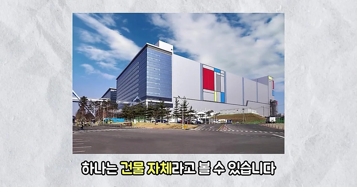
With the arrival of the AI era and the explosion of semiconductor demand, selecting locations to build semiconductor manufacturing facilities, known as 'Fabs', has emerged as a national task. This is because, beyond simply securing large plots of land, these sites must satisfy the most demanding conditions among all human-made structures. According to a video from Unrealscience, a semiconductor factory is a special facility that must simultaneously satisfy four extreme conditions: dust, vibration, water, and electricity.
Dust and Vibration Threatening Nanometer Processes, and 'Ultra Pure Water'
The line width of semiconductor circuits is measured in nanometers (nm), which is about 1/100,000th the thickness of a human hair. If even a single grain of dust settles on these microscopic circuits, an entire wafer is treated as defective. Considering that the price of a single wafer exceeds tens of millions of won, a single grain of dust directly leads to massive economic losses. To prevent this, a 'cleanroom' is essential in the factory. A 'Class 1' cleanroom, the highest grade, must maintain one or fewer particles of 0.5 micrometers or larger per cubic foot of space. This is about 99.9998% lower than the particle concentration in a typical office (approximately 500,000 particles). Engineers wear dustproof suits similar to spacesuits to block dead skin, fabric debris, and even particles in their breath. The cleanroom area of a modern Fab must be maintained 24 hours a day, spanning the size of 15 to 30 soccer fields.
Vibration control is also a matter of survival. Lithography equipment, which draws nanometer-scale circuits, uses light to engrave circuits; because the precision is so extreme, even the vibration from a large truck passing near the factory can cause errors. To prevent this, independent vibration isolation platforms separated from the building floor are installed, or active vibration isolation devices that use air pressure or electromagnetic force to slightly levitate the equipment are used. However, as seen in the case of Kumamoto, Japan, natural disasters are difficult to control through technical preparation alone. Following the shutdown of a nearby Sony factory during a magnitude 7.3 earthquake in 2016, a magnitude 7.1 strong earthquake in July 2026 caused TSMC's first plant to stop operations and evacuate employees, and even halted the construction of the second plant. Earthquake vibrations are a fatal risk that requires re-inspecting all equipment.
The 'water' at the core of the process is also special. The semiconductor process uses 'Ultra Pure Water', which reduces impurities to 1/10,000th the level of tap water (10ppb or less). Compared to the impurity concentration of tap water, which is about 100ppm (one part per million), it is in an extremely purified state. Ultra Pure Water goes through three stages: pre-treatment (filtration and reverse osmosis), pure water manufacturing (degassing, UV oxidation, ion exchange), and water quality adjustment, a process similar to a massive chemical plant. If four Fabs are operated, the daily consumption reaches approximately 650,000 tons, which is comparable to the daily water supply of a major metropolitan city.
Limits of Power Infrastructure and the Value of 'Power Inner Regions'
The most decisive variable is electricity. As the AI era begins in earnest, energy demand has surged to the point where the power required for a single ChatGPT query is about 10 times that of a Google search. The power consumption of the semiconductor Fabs that make AI chips is also enormous. The power required for four Fabs is approximately 6.3 gigawatts (GW), which, when converted to an annual basis, is comparable to the total electricity consumption of all citizens in Seoul. As seen in the case of Intel's Ohio Fab, it typically takes 7 to 9 years just to build core utility infrastructure, such as power plants, ultra-high voltage transmission lines, substations, and redundant backups, in addition to the power plant itself. Therefore, choosing a place with abundant power from the start is key to shortening the construction period.
In this context, a military runway site in Gwangju, Jeollanam-do, is recently being discussed as a candidate site for a semiconductor factory worth approximately 800 trillion won. 800 trillion won is about 10% larger than the South Korean government's annual budget for 2026 (approximately 728 trillion won). Since the runway is already leveled and wide (approximately 2.5 million pyeong) for fighter jet operations, site preparation time can be reduced. Additionally, the fact that no earthquake of magnitude 4.0 or higher has occurred in the region for the past 25 years is advantageous in terms of vibration control. Regarding water supply, it is reported that the total storage capacity of the 8 dams in the Seomjin River and Yeongsan River water systems (approximately 1.5 billion tons) can handle the daily demand of 650,000 tons if regulated. As for electricity, the self-sufficiency rate of the Gwangju and Jeollanam-do region is about 170%, making it a 'Power Inner Region' that produces 70% more electricity than the local consumption. The government is planning to build 345kV transmission lines and substations with the goal of supplying 3.1GW in the first stage and a cumulative 6.3GW in the second stage.
The Gap Between Technical Potential and Realistic Challenges
Cases where military facilities have transformed into high-tech industrial hubs can be found in Silicon Valley and the Hsinchu Science Park in Taiwan. Silicon Valley started from a hub for military electronic equipment and radar research at Stanford University during World War II, and Hsinchu, the home of TSMC, was also a military city for reconnaissance missions against China during the Cold War. The Gwangju Military Airport Project follows this trend, but there are many mountains to climb for success. First, there is an analysis that 12 out of 34 345kV transmission lines in the Honam Region are expected to reach their capacity limits before 2030, making the securing of stable power supply a key issue. Furthermore, questions are being raised about whether a power supply centered on renewable energy is suitable for semiconductor processes that require uninterrupted power.
The issue of securing water resources is also a variable. Considering the record-breaking 281-day drought experienced by the Gwangju and Jeollanam-do regions in 2022–2023, additional verification is needed to see if 650,000 tons of water per day can be stably supplied amidst climate change. The fact that the Juam Dam water level remained at 56% as of August this year is also a factor to consider. Finally, due to the nature of military facilities, detailed geological surveys are not made public, leaving uncertainty as to whether the runway ground can meet the vibration control standards for nanometer-scale processes. If this plan succeeds, the regional economic ecosystem could undergo a complete transformation, similar to Kumamoto, Japan, where TSMC is located. In the case of Kumamoto, the population has increased by more than 500 people every year since TSMC moved in, and an economic ripple effect of approximately 180 trillion won is expected by 2036. Gwangju and Jeollanam-do also have plans to nurture approximately 23,000 semiconductor workers in connection with local universities.



Comments 0